As electronic components get smaller and more complex, traditional stencil printing methods are struggling to keep up. In this blog, we explore how solder paste jet printing offers a more precise, flexible, and efficient solution — improving yields, reducing delays, and addressing common manufacturing challenges.
The challenge
Engineers are faced with continuing reductions in the size of electronic components, creating designs that are increasingly challenging to assemble to printed circuit boards (PCBs). These components need ever decreasing amounts of solder to be precisely applied as a key parameter to ensure acceptable manufacturing yields.
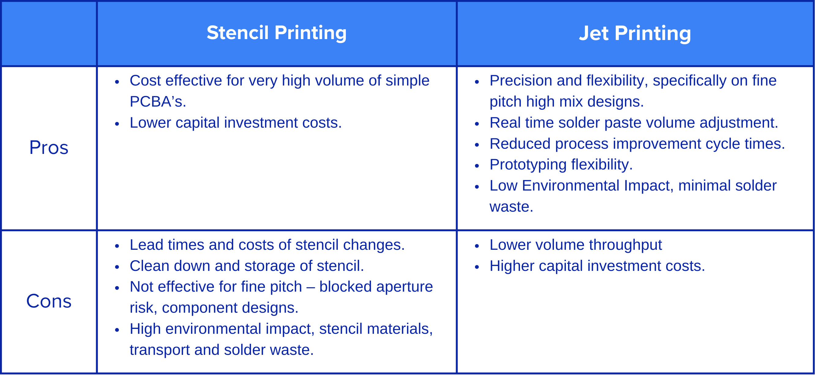
The well-established method for applying solder to a PCB uses a stencil, typically made of metal, with precise apertures aligned with the PCB pad, which allows solder to be accurately transferred to the board. These stencils are expensive to manufacture, with precision laser cut apertures and several weeks lead time, creating potential delays in the manufacturing cycle. Even with optimised processes it is commonly reported this stencil printing process accounts for 50—70% of solder defects[1][2].
The solution: Solder Paste Jet Printing
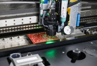
Jet Printing is a unique additive process that applies single solder ‘dots’ to deposit the exact required quantity of solder from cartridges, in the exact place needed for each component on a PCB. The ‘dot’ sizes are defined within software, from 0.2mm to 0.58mm diameter and dispensed through a nozzle, that rapidly travels across the PCB and has the capacity to place 1 million dots in an hour. Jet printing allows a software controlled near real time adjustment of the solder volume applied to each pad and thus the process improvement times are very fast. It requires no additional tooling of stencils and thus eliminates any process setup delays that may occur if new stencils are required. These capabilities excel for fine pitch designs and complex pad geometries.
Additional benefits of Solder Paste Jet Printing
With a Jet Printer, during prototype builds, board revisions and process tuning for acceptable yields, solder deposits can be adjusted in real time. This means no extra costs attributable to new stencils and the associated time delays to get these manufactured and shipped. When using a stencil printer staff need to monitor the solder paste during production to ensure it is replaced before it dries out and causes potential defects, which could affect yield further down the manufacturing process. These risks can be removed from the process by utilising Jet Printing technology.
Jet printers also have automated optical inspection of solder paste deposits before releasing the PCB to subsequent production processes. During this inspection any out of specification paste deposit will automatically be repaired without the need for manual intervention, thus resulting in higher yields.
Environmental and health and safety concerns are also improved compared to stencil printing. There is no need to process any steel or carry out laser cutting, and no need to freight stencils across the world. With Jet Printing, solder paste does not need to be directly handled, it is supplied in cartridges that are installed into the Jet Printer. These factors also have the advantage of minimising solder waste, there is no requirement to clean down the excess solder on the stencil and no requirements to store stencils when not in use and can take up appreciable space Thus, optimum material usage, floorspace reduction and cost.
Investment in this technology has allowed ASL to provide customers with reduced cost and lead times. For prototype builds and all production volumes its’ capability allows ASL to provide assembly of more complex and fine pitch geometry components with benefits in lead times and yields, with environmental and health and safety advantages.
Curious?Reach out and come to see the only one in a contract manufacturer in New Zealand.